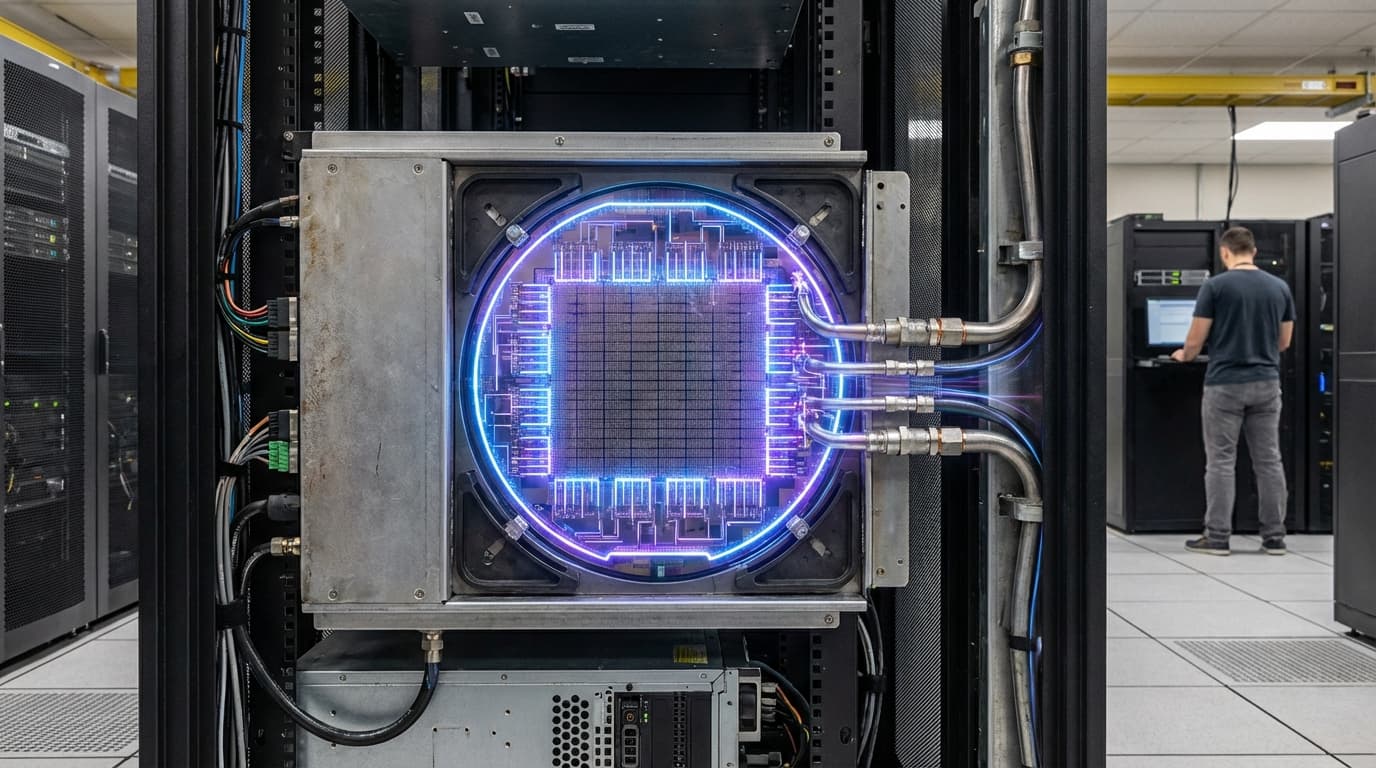
Wafer-Scale AI Systems
Wafer-scale AI systems use entire silicon wafers (typically 12 inches in diameter) as single, monolithic compute chips rather than cutting them into individual dies. This approach eliminates the need for off-chip communication between separate processors, enabling massive on-wafer memory bandwidth and parallelism that can support trillion-parameter AI models. Companies like Cerebras have commercialized these systems, creating the largest chips ever built with hundreds of thousands of cores and massive on-chip memory.
This innovation addresses the communication bottleneck that limits the scale of AI systems, where moving data between chips becomes a major constraint for large models. By keeping everything on a single wafer, these systems can achieve unprecedented memory bandwidth and reduce latency, enabling training and inference of models that would be impractical with traditional multi-chip systems. The technology is already deployed in some of the world's largest AI research facilities and cloud providers.
The technology is particularly significant for training frontier AI models that require massive scale, where communication overhead can dominate training time. As AI models continue to grow in size and complexity, wafer-scale systems offer a pathway to scaling that avoids the communication bottlenecks of multi-chip systems. However, the technology faces challenges including manufacturing yield (defects on large wafers), power density, and cost, which limit its applicability to the largest, most demanding AI workloads.
Related Organizations

Developer of the Wafer Scale Engine (WSE), the largest computer chip ever built, designed specifically for AI compute.
Taiwan Semiconductor Manufacturing Company (TSMC)
Taiwan · Company
Global semiconductor foundry leader providing the advanced manufacturing and packaging processes required for wafer-scale integration.

UAE-based AI and cloud computing company building massive supercomputers.

Argonne National Laboratory
United States · Research Lab
U.S. Department of Energy multidisciplinary science and engineering research center.
United States · Company
Cloud services provider specializing in deep learning infrastructure.

Federal research facility focusing on national security and nuclear science.

Saudi Arabia · University
Private research university in Saudi Arabia.

Automotive and energy company developing custom AI silicon for autonomous driving.


Broad energy company producing and marketing energies on a global scale.
Supporting Evidence
Research this in Signals
Signals turns a topic into a sourced research record you can inspect and rerun. Your first scan is free, and this one starts with Wafer-Scale AI Systems already loaded, so edit it or scan as is.