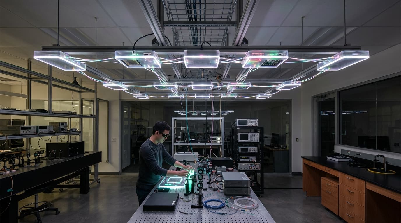
Photonic Integrated Circuits (PICs)
Photonic Integrated Circuits represent a fundamental shift from electronic to optical signal processing, leveraging the unique properties of light to perform functions traditionally handled by electrical circuits. Unlike conventional silicon-based electronics that rely on electron flow, PICs manipulate photons—particles of light—to transmit, process, and detect information. These chips integrate multiple optical components including laser sources, waveguides, modulators, photodetectors, and filters onto a single substrate, typically using materials like silicon, indium phosphide, or silicon nitride. The core principle involves confining and routing light through microscopic waveguides etched into the chip surface, enabling complex optical operations within a footprint measured in millimeters. This integration allows for the miniaturization of what would otherwise require bulky optical benches and discrete components, while simultaneously reducing power consumption and improving reliability through the elimination of numerous optical connections and alignments.
The integration of PICs into lighting infrastructure addresses several critical limitations in modern urban environments and industrial settings. Traditional lighting systems serve a single purpose—illumination—while consuming significant energy and occupying valuable real estate without contributing to data infrastructure or environmental monitoring. By embedding photonic circuits directly into luminaires, these systems transform passive light sources into active nodes within a broader sensing and communication network. This convergence solves the bandwidth limitations of radio-frequency wireless systems through Li-Fi technology, which can achieve data transmission rates orders of magnitude faster than Wi-Fi by modulating visible light at imperceptible frequencies. Simultaneously, the same hardware enables precise distance measurement and object detection through integrated LIDAR functionality, eliminating the need for separate sensor installations. The computational capabilities embedded within these photonic chips allow for real-time data processing at the edge, reducing latency and network congestion while enabling immediate responses to detected conditions such as occupancy changes, air quality variations, or security events.
Early deployments of photonic-integrated lighting systems have emerged in smart building environments and industrial facilities where high-bandwidth communication and precise spatial awareness justify the initial investment. Research institutions and technology companies are exploring applications ranging from indoor positioning systems with centimeter-level accuracy to adaptive lighting that responds to real-time environmental conditions and occupant behavior. The technology shows particular promise in settings where electromagnetic interference prohibits traditional wireless communication, such as hospitals, manufacturing plants, and data centers. As fabrication techniques mature and economies of scale reduce production costs, industry analysts anticipate broader adoption across commercial real estate, transportation infrastructure, and eventually residential applications. The convergence of lighting, communication, and sensing within a single photonic platform aligns with broader trends toward multifunctional infrastructure and the densification of urban sensor networks, positioning PICs as a key enabling technology for future smart cities where every light fixture serves as an intelligent node within an interconnected urban nervous system.
Related Organizations

Creates LiDAR-on-a-chip solutions using silicon photonics, enabling compact 3D sensing that can be embedded into lighting infrastructure.

A manufacturing institute dedicated to advancing integrated photonics technology, providing fabrication and packaging services.

German research institute developing advanced algorithms for 3D Human Body Reconstruction and volumetric video coding.

Develops LiFi components and systems, co-founded by the 'father of LiFi' Harald Haas.

Develops a 'clinic-on-the-wrist' platform using silicon photonics to sense biomarkers via light, applicable to health-monitoring wearables.

Develops 4D vision sensors using silicon photonics (FMCW LiDAR) for machine vision and autonomous applications.


Develops silicon spin qubits using advanced 300mm wafer manufacturing processes.

Manufactures low-loss Silicon Nitride (SiN) Photonic Integrated Circuits (PICs) used in transducer research.

Provides an open silicon photonics platform with integrated lasers, allowing for scalable manufacturing of PICs.

Develops augmented silicon photonic circuits with integrated lasers for optical communications and 3D sensing.

An independent foundry for Indium Phosphide (InP) photonic integrated circuits, enabling chips that generate, modulate, and detect light.