Hyperspectral & Terahertz Sensing
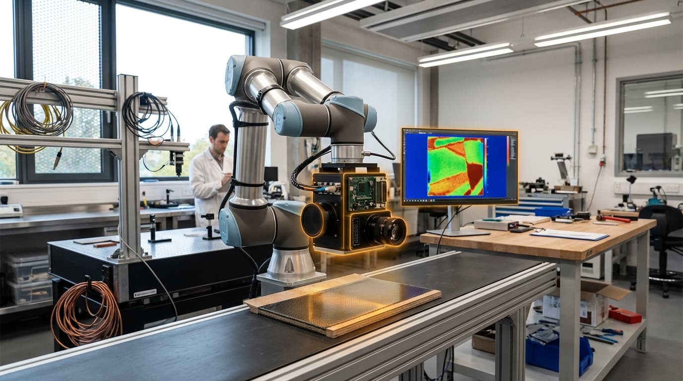
Hyperspectral and terahertz sensing technologies represent a fundamental shift in how manufacturing systems perceive and evaluate materials. Unlike conventional RGB cameras that capture only three color channels, hyperspectral imaging systems record hundreds of narrow, contiguous wavelength bands across the electromagnetic spectrum, from ultraviolet through visible light to near-infrared and beyond. Each material exhibits a unique spectral signature—a fingerprint of how it absorbs, reflects, or transmits different wavelengths—allowing these sensors to identify chemical composition, detect surface coatings, and reveal contaminants that remain completely invisible to human vision or standard cameras. Terahertz imaging operates in a different portion of the spectrum, between microwave and infrared frequencies, where electromagnetic waves can penetrate non-conductive materials like plastics, ceramics, polymers, and composite structures. This penetration capability enables the detection of internal defects such as voids, delamination, moisture intrusion, and density variations without the safety concerns and regulatory requirements associated with X-ray systems. The combination of surface-level chemical analysis from hyperspectral sensors and subsurface structural inspection from terahertz systems creates a comprehensive, non-contact quality assessment capability.
Manufacturing industries face mounting pressure to ensure product quality while maintaining high throughput and minimizing waste. Traditional inspection methods often require destructive sampling, where products are removed from production lines and physically tested, or contact-based measurements that can damage delicate components and slow production rates. These limitations become particularly problematic when dealing with high-value materials like carbon fiber composites, pharmaceutical tablets, or food products where contamination risks must be minimized. Hyperspectral and terahertz sensing address these challenges by enabling 100% inline inspection without physical contact or product destruction. In pharmaceutical manufacturing, these technologies can verify the correct distribution of active ingredients in tablets, detect coating uniformity, and identify counterfeit products—all at production speeds. For advanced composite manufacturing in aerospace and automotive sectors, they reveal manufacturing defects like fiber misalignment, resin-rich areas, or porosity that could compromise structural integrity, catching problems before expensive components enter service. The ability to inspect every item rather than relying on statistical sampling fundamentally changes quality assurance economics and risk profiles.
Research deployments and early commercial systems are already demonstrating the practical value of these sensing modalities across multiple manufacturing domains. Food processing facilities are implementing hyperspectral systems to detect foreign materials, assess ripeness uniformity, and verify ingredient authenticity in ways that traditional metal detectors and visual inspection cannot match. In electronics manufacturing, terahertz imaging reveals hidden solder joint defects and delamination in multilayer circuit boards without the throughput limitations of X-ray inspection. The pharmaceutical industry has shown particular interest, with pilot programs using these technologies for tablet coating verification and blister pack inspection to ensure product integrity. As sensor costs decline and processing algorithms become more sophisticated through machine learning integration, these technologies are transitioning from laboratory curiosities to production-floor tools. The convergence of hyperspectral and terahertz sensing with automated manufacturing systems and robotic handling represents a broader industry trend toward zero-defect manufacturing, where comprehensive material characterization becomes an integral part of production rather than a separate quality control step. This evolution promises to reduce waste, improve product consistency, and enable the manufacture of increasingly complex materials and structures that current inspection methods cannot adequately verify.
Related Organizations
A global leader in hyperspectral imaging instrumentation and systems, now part of Konica Minolta.

Develops terahertz instruments and solutions, originally for imaging but increasingly relevant for comms material characterization.

Designs and manufactures high-performance hyperspectral imaging systems for remote sensing and industrial machine vision.

Conducts advanced research into cryogenic CMOS and quantum computing interconnects.

A leading developer and supplier of instrumentation for high-precision metrology.

Develops intelligent hyperspectral imaging solutions that combine hardware with embedded logic to classify materials in real-time.

Uses hyperspectral imaging specifically for the food processing industry to detect foreign objects and assess meat quality.


A major manufacturer of digital imaging components, including specialized line-scan cameras used for multispectral and hyperspectral inspection.

Develops tunable Fabry-Perot filters (MEMS) that turn standard cameras into hyperspectral sensors.