Semiconductor Mega-Clusters
Geography: Asia Pacific · East Asia · South Korea
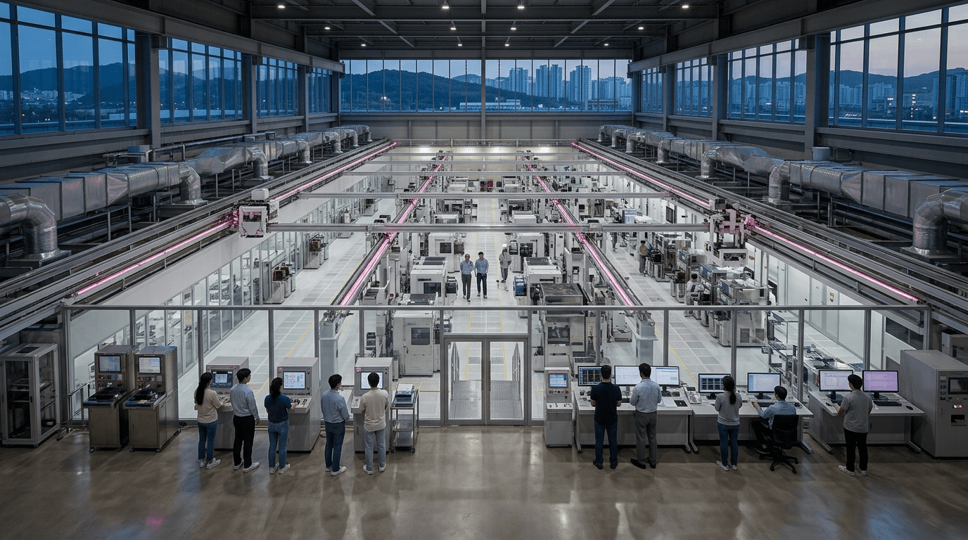
Samsung is building its P5 fab at Pyeongtaek, adding to what is already the largest semiconductor campus in the world with P1 through P4. SK Hynix broke ground on a 4.15 million square meter mega-cluster in Yongin, south of Seoul, with $91B committed through 2047. The Korean government designated a national semiconductor belt connecting these clusters with transportation, power, and water infrastructure.
These mega-clusters reflect a strategic bet that semiconductor manufacturing advantage comes from density and integration — having design, fabrication, packaging, and testing within the same campus reduces logistics costs and accelerates iteration cycles. The scale is staggering: the Yongin cluster alone will be larger than many small cities.
The geopolitical context makes these investments more urgent. With TSMC concentrated in Taiwan and US CHIPS Act funding its own fab construction, Korea is racing to ensure its semiconductor manufacturing base remains globally competitive. The Korean government's K-Semiconductor Strategy provides tax breaks of up to 25% for facility investment, explicitly designed to keep fabs in Korea rather than losing them to foreign incentive packages.