Advanced Semiconductor Packaging
Geography: Asia Pacific · East Asia · South Korea
Samsung Foundry has invested heavily in its I-Cube and X-Cube 3D packaging technologies, which stack logic and memory dies vertically using through-silicon vias and hybrid bonding at sub-1μm pitch. SK Hynix's MR-MUF (Mass Reflow Molded Underfill) packaging for HBM is already in volume production and is considered best-in-class for memory stacking.
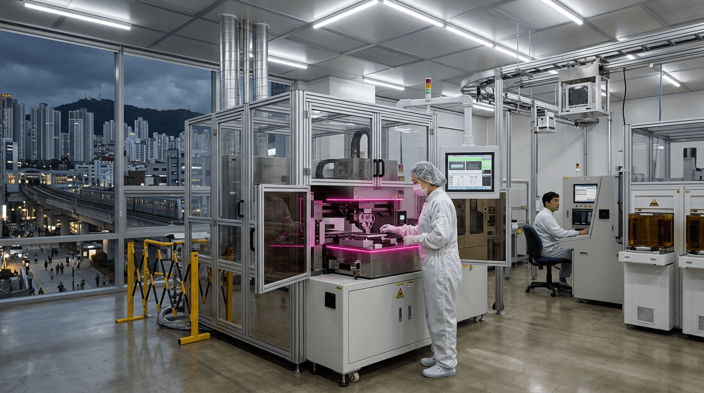
Advanced packaging has become the new battleground in semiconductors as traditional transistor scaling slows. Instead of making transistors smaller, the industry is making chips bigger by assembling multiple specialized dies (chiplets) into a single package. This requires precision bonding, thermal management, and testing capabilities that only a handful of companies worldwide possess.
Korea's position in advanced packaging is strengthened by its control of both the memory and packaging steps — SK Hynix doesn't just make HBM dies, it packages them into the final stacked product that ships to Nvidia. Samsung is positioning its packaging capabilities as a differentiator for its foundry business, competing directly with TSMC's CoWoS and InFO technologies.