Nanoimprint Lithography (NIL)
Geography: Asia Pacific · East Asia · Japan
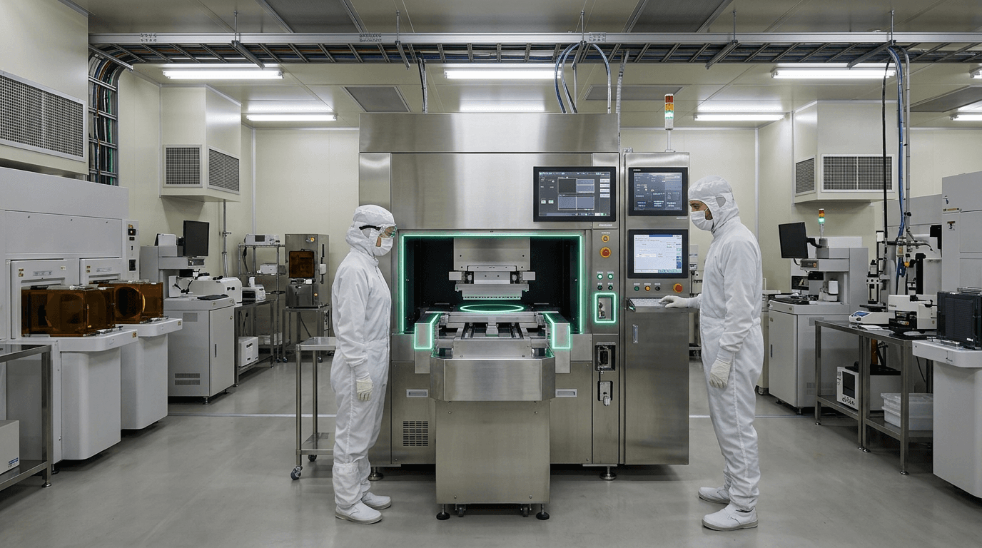
Canon Inc. has developed nanoimprint lithography (NIL) as a fundamentally different approach to semiconductor patterning. Instead of projecting light through complex optics (as ASML's EUV does), NIL physically stamps a nano-patterned mold into a resist material on the wafer — like a high-tech rubber stamp operating at the molecular level. Canon delivered its first FPA-1200NZ2C system to Toppan Inc. in 2024, demonstrating 2nm-class patterning capability. The system uses approximately 90% less power than EUV lithography and is projected to cost roughly one-tenth of an ASML EUV scanner (~$15 million vs. $150+ million).
NIL won't replace EUV for all semiconductor layers — it has lower throughput and challenges with defect density and overlay accuracy that make it unsuitable as a sole patterning technology. However, Canon's strategy is co-existence: NIL can handle specific layers (particularly memory and repetitive patterns) where its precision is sufficient and its cost advantage is enormous. This opens advanced chipmaking to smaller fabs that cannot afford $150 million EUV scanners, potentially democratizing access to sub-5nm patterning technology.
The strategic context is Japan's broader effort to reclaim semiconductor manufacturing relevance. Canon lost the lithography race to ASML in the 2010s when it bet against EUV, but NIL represents a lateral move — not competing head-on with EUV but offering a complementary technology that reduces the total cost of advanced chipmaking. If Rapidus or other Japanese fabs integrate NIL for non-critical layers alongside EUV for critical patterning, the combination could create a cost-competitive manufacturing approach. Canon's NIL also has applications beyond semiconductors: photonic devices, biomedical microstructures, and AR/VR optical elements all benefit from precise nano-patterning at low cost.