CMOS Image Sensor Technology
Geography: Asia Pacific · East Asia · Japan
Sony Semiconductor Solutions dominates the global CMOS image sensor market, with Japanese companies collectively holding approximately 48% of worldwide production. Sony's stacked CMOS sensor architecture — placing the pixel array, logic processing, and memory in separate layers bonded together — represents the most advanced image sensor design in production. These sensors power every iPhone camera, most flagship Android phones, leading autonomous vehicle perception systems (including partnerships with automotive manufacturers), and industrial machine vision applications. Sony's Kumamoto fab, adjacent to TSMC's JASM facility, produces sensors at massive scale.
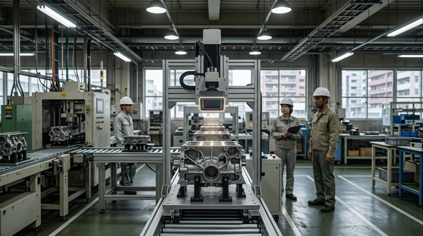
The technology extends far beyond smartphone cameras. Sony's event-based vision sensors (detecting changes rather than capturing full frames) enable ultra-low-latency perception for robotics and autonomous driving. Time-of-flight (ToF) sensors for depth mapping, SWIR (short-wave infrared) sensors for medical and agricultural imaging, and radiation-hardened sensors for space applications all represent growing segments. Hamamatsu Photonics and Canon add further Japanese depth in specialized image sensors for scientific and industrial applications.
Strategically, image sensors are becoming the primary interface between the physical world and AI systems. As autonomous vehicles, industrial robots, smart cities, and AR/VR devices proliferate, demand for increasingly capable image sensors grows exponentially. Sony's vertically integrated approach — designing both the sensor silicon and the image signal processing algorithms — creates a systems-level advantage. The proximity of Sony's sensor fab to TSMC's Kumamoto logic fab creates a semiconductor cluster that could become globally significant for AI perception hardware.