Semiconductor Design Ecosystem
Geography: Asia Pacific · South Asia · India
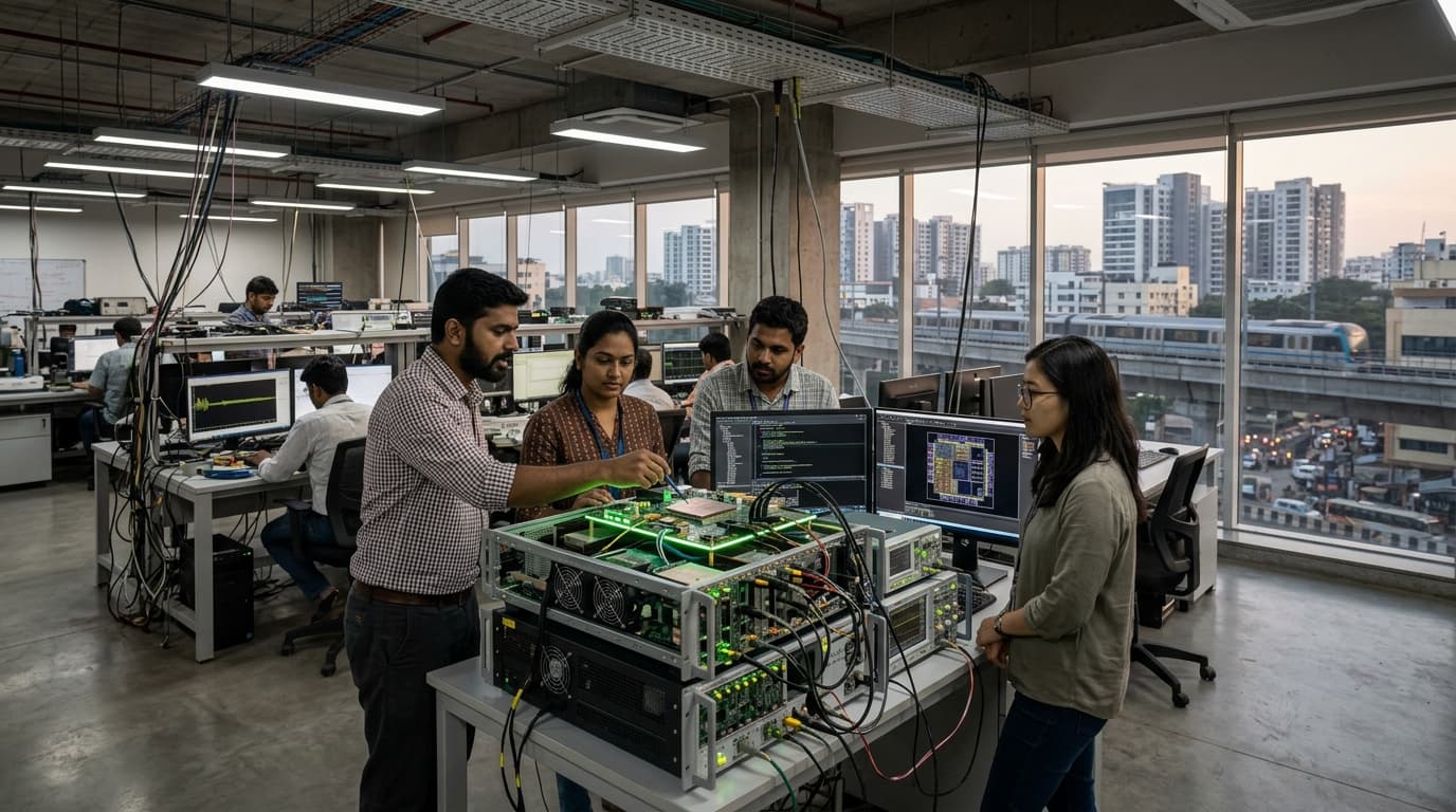
India is already one of the world's leading semiconductor design hubs, even before manufacturing capability comes online. An estimated 20-25% of global chip design work happens in India, with over 100,000 chip design engineers working across multinational R&D centers and domestic companies. Major design centers include Qualcomm India (one of Qualcomm's largest global design centers), Intel India (which has designed several generations of processors), ARM India, AMD India, NVIDIA India, and Broadcom India.
Bengaluru and Hyderabad are the twin hubs of India's semiconductor design ecosystem. Many of the ARM cores that power smartphones worldwide, the GPU architectures that enable AI training, and the 5G modem chips that enable modern connectivity were designed or co-designed in India. This represents enormous accumulated expertise in digital design, verification, and physical design — the intellectual backbone of the semiconductor industry.
The design ecosystem's maturity is India's strongest argument for why domestic fabrication can succeed. Unlike countries starting semiconductor programs from scratch, India already has the engineering talent, the design tools expertise, and the industry relationships. The missing piece is manufacturing — and the India Semiconductor Mission is specifically targeting that gap to complete the value chain.