
Envisioning is an emerging technology research institute and advisory.

LinkedInInstagramGitHub

2011 — 2026

research
  • Reports
  • Newsletter
  • Methodology
  • Origins
  • My Collection
services
  • Research Sessions
  • Signals Workspace
  • Bespoke Projects
  • Use Cases
  • Signal Scanfree
  • Readinessfree
impact
  • ANBIMAFuture of Brazilian Capital Markets
  • IEEECharting the Energy Transition
  • Horizon 2045Future of Human and Planetary Security
  • WKOTechnology Scanning for Austria
audiences
  • Innovation
  • Strategy
  • Consultants
  • Foresight
  • Associations
  • Governments
resources
  • Pricing
  • Partners
  • How We Work
  • Data Visualization
  • Multi-Model Method
  • FAQ
  • Security & Privacy
about
  • Manifesto
  • Community
  • Events
  • Support
  • Contact
  • Login
ResearchServicesPricingPartnersAbout
  1. Home
  2. Research
  3. Forge
  4. Advanced Semiconductor Packaging (CoWoS, Foveros)

Advanced Semiconductor Packaging (CoWoS, Foveros)

TSMC's CoWoS and Intel's Foveros 3D packaging technologies stack chiplets and high-bandwidth memory into integrated packages, becoming the key bottleneck in AI chip supply — CHIPS Act funds dedicated US packaging facilities.
Back to ForgeView interactive version

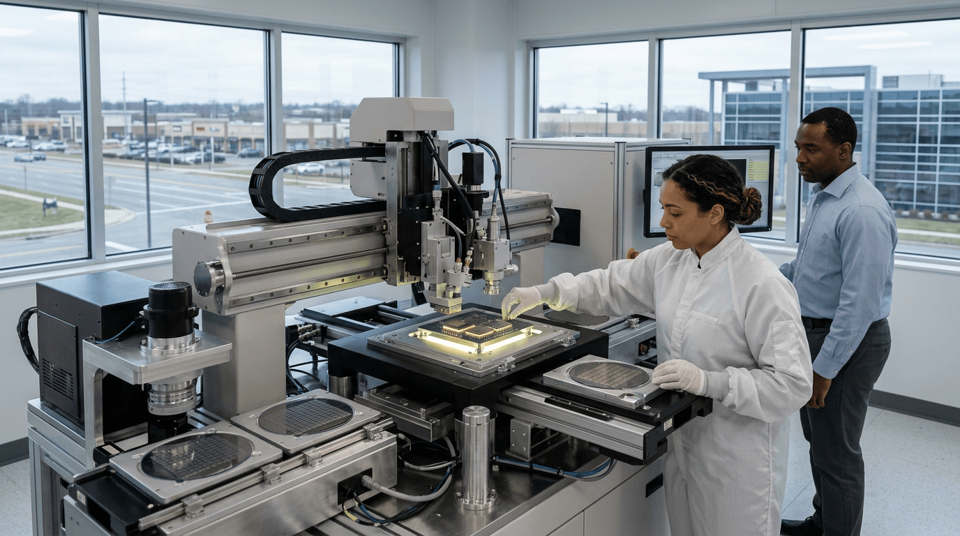
Advanced semiconductor packaging integrates multiple dies (chiplets, memory, interconnects) into a single package using technologies like TSMC's Chip-on-Wafer-on-Substrate (CoWoS) and Intel's Foveros. These packages combine compute chiplets with high-bandwidth memory (HBM) stacks, enabling the massive memory bandwidth that AI accelerators require. NVIDIA's H100 and B200 use CoWoS packaging.

Advanced packaging has become the critical bottleneck in AI chip supply — TSMC's CoWoS capacity limits how many AI GPUs can be produced, regardless of wafer fabrication capacity. This has made packaging technology as strategically important as lithography. The CHIPS Act includes specific funding for advanced packaging R&D and manufacturing facilities in the US.

Packaging innovation is where the US can build domestic capability without replicating TSMC's leading-edge wafer fabrication. Intel's US-based packaging facilities, combined with CHIPS Act-funded research, could create a domestic advanced packaging ecosystem that adds value even when bare dies are fabricated overseas.

TRL
8/9Deployed
Impact
4/5
Investment
5/5
Category
Hardware

Book a research session

Bring this signal into a focused decision sprint with analyst-led framing and synthesis.
Research Sessions