Atomically Precise Manufacturing
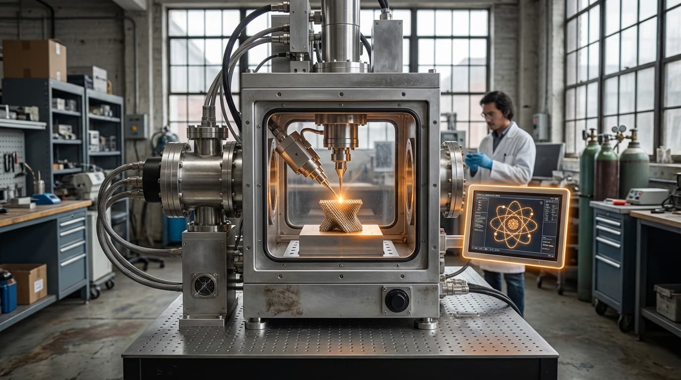
Atomically Precise Manufacturing represents a paradigm shift in how we conceive and execute the production of materials and components. Unlike conventional manufacturing processes that work with bulk materials and accept inherent imperfections, APM seeks to control matter at the most fundamental level—positioning individual atoms or molecules with nanometer-scale precision to construct larger structures. This approach builds upon advances in scanning probe microscopy, molecular self-assembly, and computational chemistry to enable the deliberate arrangement of matter atom by atom. The technical foundation relies on several complementary methods: mechanosynthesis uses molecular-scale tools to place atoms in specific locations, while directed self-assembly guides molecules to organize themselves into predetermined patterns. DNA origami and protein engineering provide biological pathways for atomic-scale construction, and advanced lithography techniques continue to push the boundaries of what can be patterned at near-atomic resolutions. The fundamental principle is that by controlling structure at the atomic level, manufacturers can achieve materials and devices with properties that approach theoretical physical limits.
The manufacturing sector has long grappled with the trade-off between precision and scale, along with the inevitable defects that arise from working with imperfect materials and processes. Even the most advanced semiconductor fabrication facilities operate at tolerances measured in nanometers but cannot yet control individual atomic positions across entire products. APM addresses these limitations by promising materials with zero structural defects, eliminating the weak points that cause mechanical failures and the impurities that degrade electronic performance. This capability would enable the creation of aerospace components with strength-to-weight ratios that match theoretical maximums, potentially reducing aircraft weight by orders of magnitude while maintaining or improving safety margins. In electronics, atomically precise conductors and semiconductors could operate at the physical limits of electrical and thermal performance, dramatically improving energy efficiency in everything from data centers to consumer devices. The energy sector stands to benefit from perfect photovoltaic materials that capture sunlight with unprecedented efficiency and battery electrodes with optimal surface area and conductivity.
Current research in atomically precise manufacturing remains largely confined to laboratory demonstrations and highly specialized applications. Researchers have successfully manipulated individual atoms using scanning tunneling microscopes and created small molecular machines that perform basic mechanical operations. The semiconductor industry's ongoing pursuit of smaller transistors has driven investment in atomic-layer deposition and other techniques that approach atomic precision in thin-film manufacturing. However, scaling these capabilities from laboratory curiosities to industrial production presents formidable challenges in throughput, cost, and process control. Early commercial applications are likely to emerge first in high-value sectors where the premium for perfect materials justifies extensive processing time—specialized sensors, quantum computing components, and medical devices represent promising initial markets. As the technology matures, it connects to broader trends in advanced manufacturing, including the integration of artificial intelligence for process optimization and the development of hybrid approaches that combine top-down lithography with bottom-up molecular assembly. The trajectory suggests a gradual transition rather than an immediate revolution, with atomically precise techniques first augmenting conventional manufacturing before potentially transforming entire industries over the coming decades.
Related Organizations
Focuses on atomically precise manufacturing, a prerequisite for constructing theoretical reversible mechanical computing systems.
Nonprofit advancing beneficial nanotechnology and molecular manufacturing.

Manufacturer of high-precision lithography systems, including the NanoFrazor.

Long-standing leader in neuro-symbolic AI, combining neural networks with logical reasoning for enterprise applications.

An investment entity focused on advancing nanotechnology and molecular manufacturing.

Manufactures ultra-sharp probes for atomic force microscopy and atomic precision.

Runs the Semantic Forensics (SemaFor) program to develop technologies for automatically detecting, attributing, and characterizing falsified media.

The US federal agency leading the global competition to select and standardize post-quantum cryptographic algorithms.

Leads the DISCOVERER project focusing on VLEO aerodynamics and materials.